Tesla Semiconductor In-House Manufacturing — Eliminating the 60% Wafer Idle-Time Problem
Published · Updated · By Investus editorial desk (SUNRYU Partners)
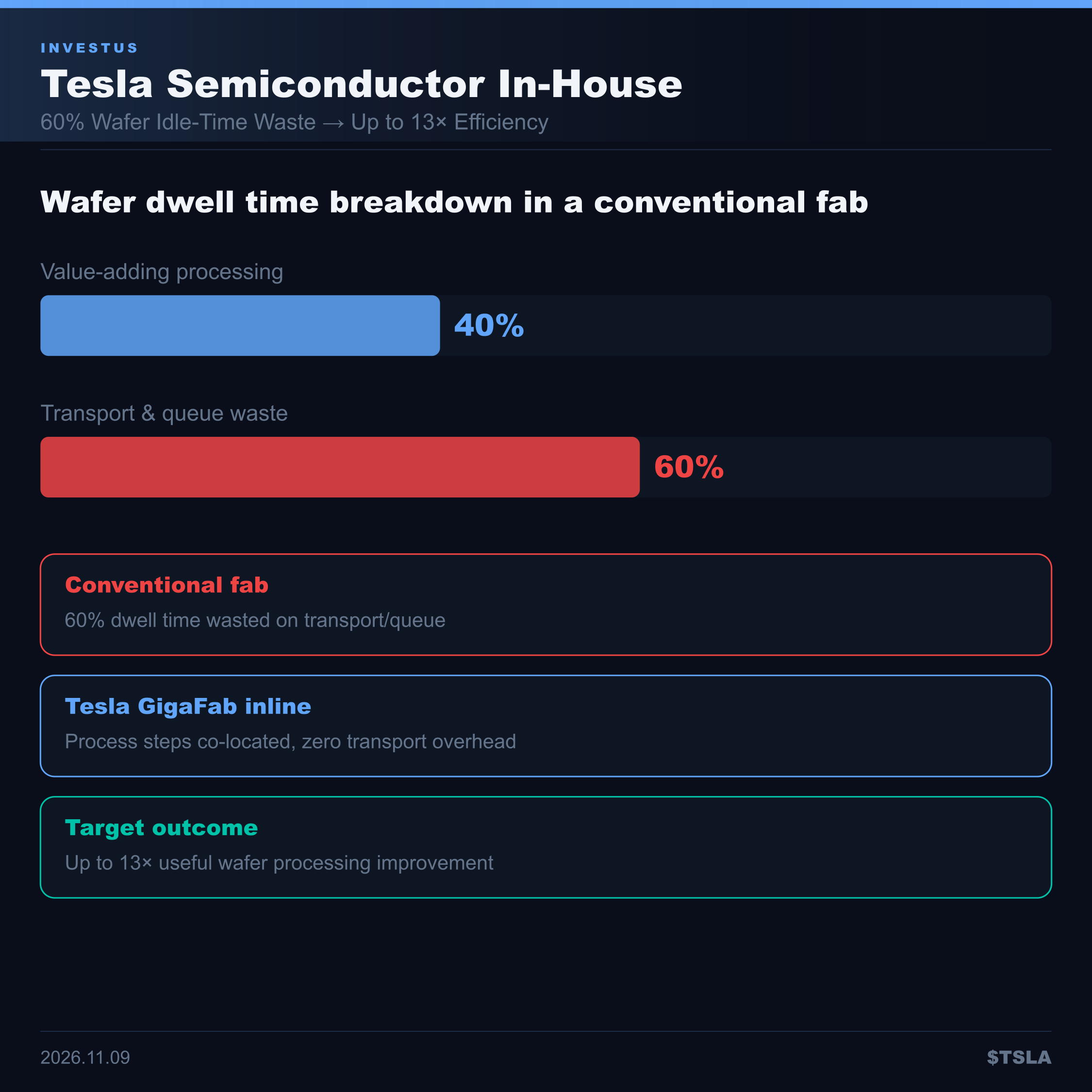
Tesla is pursuing a first-principles redesign of semiconductor manufacturing. Conventional fabs waste approximately 60% of wafer dwell time on transport and queues between machines. Tesla's inline GigaFab concept aims to eliminate this waste and achieve up to 13× improvement in useful wafer processing time.
What happened
Tesla is developing an approach to fundamentally change how semiconductor wafers are manufactured. In a conventional fab, a wafer passes through hundreds of process steps, but only about 40% of its time is spent in value-adding processing — roughly 60% is wasted on transport between tools and queue time. Tesla's 'GigaFab inline' concept targets eliminating this waste, with researchers estimating up to 13× improvement in useful processing time could be achievable.
Existing fabs have structural limitations baked in. A single wafer takes 3–6 months to become a finished chip; in large fabs with complex logic products, cycle times can be even longer. Pure processing time — the days actually adding structure to the wafer — is a small fraction of that total cycle. Tesla's approach is to co-locate process steps in-line, eliminating transport overhead entirely.
More detail
Semiconductor fabs are extraordinarily capital-intensive — TSMC's latest 2nm fab requires more than $20 billion in upfront investment. If Tesla operates its own fab, it reduces dependence on external foundries and allows tighter integration between Terafab AI chip design and manufacturing. This is Musk's first-principles method applied to semiconductors: challenge conventional practice, redesign from physics up.
Today Tesla's semiconductor operations center on the FSD HW4 chip (manufactured by Samsung Foundry). An inline GigaFab could eventually produce automotive AI chips, Terafab AI accelerators, and Optimus robot control chips from a single vertically integrated line. Heavily automated, near-zero labor and transport overhead aligns with Tesla's manufacturing philosophy.
Analyst and house views
Tesla's semiconductor in-sourcing program is in early stages and is not yet formally incorporated into major house price targets. However, Wedbush estimates that Tesla producing 50%+ of its key FSD, robotaxi, and Optimus chips in-house by 2028 could add $3–5 to EPS. If in-house manufacturing is realized, Tesla's valuation case shifts further from pure automaker toward an AI hardware-software integrated platform.
investus Research
Sources & further reading
Related Guides
Related articles
Anthropic's $120.5B SpaceX Compute Deal: What the 90-Day Exit Clause Means After the 'Mid-2027' Report
Anthropic's S-1/A caps SpaceX compute at $120.5B with a 90-day exit after early 2027. What the 'mid-2027' report adds and what remains unconfirmed.
35,578 Open Grok Build Apps: What Claroc Measured and What SpaceXSI Disputes
SpaceXSI's Grok Build: Claroc says 35,578 published apps opened with no sign-in. What was measured, what SpaceXSI disputes, and open questions.
Starship Flight 15 Explained: SpaceX's First Attempt to Catch Both Stages, What Is Confirmed and What Investors Should Watch
SpaceX says Starship Flight 15 is preparing to launch as soon as Friday, November 13, 2026, pending regulatory approval, on the first plan to catch both Super Heavy and the Starship upper stage. The 75-minute window opens at 4:45 p.m. CT. This note separates confirmed facts, company plans, secondary reports, and open questions. It is not a buy, a sell, or a share-price call.
Disclaimer
This article is editorial research for informational purposes only. It is not investment advice, a recommendation, or a solicitation to buy or sell any security, and does not guarantee any return. Markets carry risk of loss. Verify figures against the primary sources before making decisions.